| | 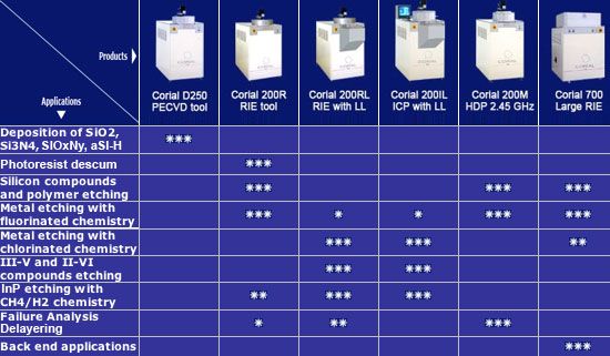  | Manually loaded RIE system controlled by PC with software operating under Linux. It uses fluorinated reactive gases for Si, SiO2, Si3N4, SiC, Ge, W, Ta, Ti, TiN, Nb, Mo and polymer etching. When equipped with a CCD camera laser endpoint detector, it offers automatic multistep process capability. | | |  | Manually loaded RIE system with vacuum load-lock for up to Ø200 mm substrates. It is controlled by PC with software operating under Linux. It uses CH4/H2 and chlorinated reactive gases for etching of III-V and II-VI compounds like GaAs, GaAlAs, InP, InGaAsP, ZnS, CdTe and HgCdTe. When equipped with a CCD camera laser endpoint detector, it offers automatic multistep process capability. | | |  | Manually loaded High Density Plasma system controlled by PC with software operating under Linux. It operates in High Density Plasma and RIE mode for deprocessing of either packaged dies, dies or wafers up to Ø200 mm. When equipped with a CCD camera laser endpoint detector, it offers automatic multistep process capability. | | | 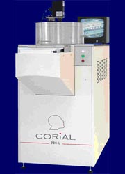 | Manually loaded ICP system with vacuum load-lock for up to Ø200 mm substrates. It is controlled by PC with software operating under Linux. It uses CH4/H2 and chlorinated reactive gases for etching III-V and II-VI compounds like GaN, GaAs, GaP, GaAlAs, InP, InGaAsP, ZnS, CdTe and HgCdTe. When equipped with a CCD camera laser endpoint detector, it offers automatic multistep process capability. | | | 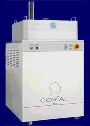 | Manually loaded RIE system with very large cathode area (substrate size up to 650 mm X 600 mm). It uses fluorinated and chlorinated chemistry for the etching of materials like Si, aSi-H, SiO2, Si3N4, W, Ta, Ti, Nb, Mo, Cr and polymers. It is controlled by PC with software operating under Linux. When equipped with a CCD camera laser endpoint detector, it offers automatic multistep process | | | 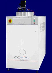 | Manually loaded PECVD with high temperature isothermal reactor inside a vacuum vessel. It is controlled by PC with software operating under Linux. It is dedicated to fast deposition of aSiH, Si3N4, SiO2 and silicon oxi-nitrides on wafers up to Ø200 mm. When equipped with a CCD camera laser endpoint detector, it offers automatic multistep process capability. | |